Micro- and Nano- Fabrication


I have always loved the multidisciplinary nature of micro- and nano-fabrication. The nanofab truly tests a scientist's general understanding of how the universe ticks in a way that has very real consequences in terms of ruined samples and wasted days. To be effective, one needs a working knowledge of optics, mechanics, physics, material science, and chemistry. Furthermore, one needs excellent soft-skills in managing the trouble-shooting process and making the most out of the information every sample (no matter how far from desired) gives you.
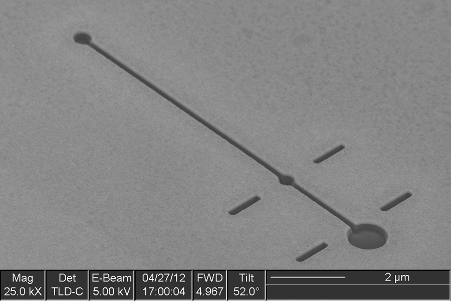
Top-Down Fabrication
I have experience with optical lithography, electron beam (e-beam) lithography, and Focused Ion Beam (FIB) lithography. I have experience with thermal and electron beam evaporation. I have experience with wet etching, reactive ion etching, and XeF2 etching.
Bottom-Up Fabrication
I have built a setup for fabricating metallic nanowires using the alumina-templated electrodeposition technique. I have also built a setup for creating alternating metal-dielectric layers using self-oscillatory pH levels. I worked with electrospinning nanofilaments.
Characterization
I have with scanning electron microscopy (SEM), atomic force microscopy (AFM), profilometry, optical profilometry, reflectometry, and ellipsometry.