- Edwards BE, Rubin N, and Engheta N. Gordon Research Conference - Plasmonics. "Experimental Measurements of Suspended MIM Waveguides and Dipole & Cavity Plasmonic Waveguide Couplers"
- Edwards BE, and Engheta N. 2014 Conference on Lasers and Electro-Optics (CLEO), San Jose. "Suspended MIM optical waveguides with optical nano-antennas"
Uvula Antennas and Plasmonic Slot Waveguides
Brian Edwards, Noah Rubin, Nader Engheta
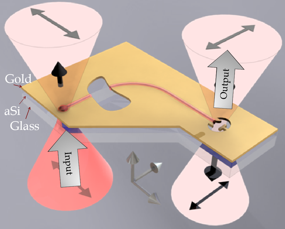
Schematic of the experimental setup consisting of two antennas connected using a suspended MIM plasmonic waveguide. Input antenna is illuminated from below and the light travels to the output antenna where it is radiated with an orthoganal polarization.
SEM of a typical sample wherein each waveguide is identical with the exception of its length.
In this largely unpublished work, we fabricated plasmonic "slot" (aka MIM) waveguides. Our goal was to measure the complex transmission through these waveguides with an NSOM. These results were to serve a greater purpose that was never realized, however, I believe the part of the road that was traveled was interesting enough to warrant discussion here.
In a plasmonic slot waveguide, the waveguide mode is confined between two plasmonic mediums (metals). This is very different from a traditional optical waveguide which is made out of various glasses (dielectrics). In this way, it has more in common with the power cord on your bedside lamp than it does an optical fiber. Similar to a power cord, the plasmonic waveguide is more tolerant of bends than a traditional optical waveguide.
Just as certain metals are better for conducting electricity (ie copper and aluminum), certain metals are better at conducting light. Gold and silver are the most popular choices. Light, apparently, has expensive taste. However, the fundamental challenge of plasmonics is that the materials are "lossy," meaning the light is quickly turning into heat as it travels down the length of the waveguide. It is not uncommon for the power to decrease by half for every several tens of microns traveled. This creates very challenging experimental constraints.
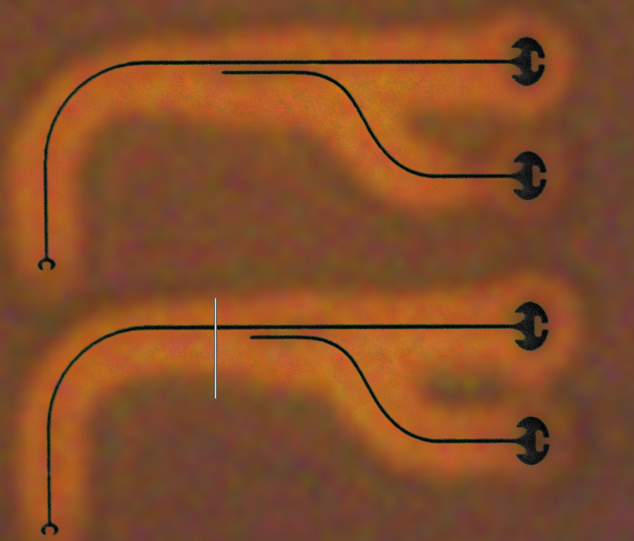
Couplers imaged from the underside with the FIB pattern superimposed in black. The line on the image is 2μm long. It can be seen that the aSi was etched back from the slot waveguide structure.
Given that our goal was to probe these waveguides with an NSOM, the waveguides could not be encapsulated with a dielectric. Modal simulations indicated that if they were fabricated on glass, the majority of the power would be contained within the glass and also be inaccessible. Therefore, we built the waveguides such that they were free-standing. This was achieved through the following fabrication steps:
- Begin with #1.5 glass coverslips
- Deposit about 300nm of amorphous Silicon (aSi) via Plasma Enhanced Chemical Vapor Deposition (PECVD)
- Evaporate about 100nm of gold via an electon beam evaporator
- Pattern the gold using Focused Ion Beam Lithography (FIBL)
- Etch the aSi using a high pressure, low power SF6 RIE.
This created free-standing gold slot waveguides with clear optical access from both above and below. We patterned an input nano-antenna at one end of the waveguide and an output nano-antenna at the other. Given the heavy losses incurred within the slot waveguide, the primary challenge of the experiment was to see the light coming from the exit antenna over the glare from the input antenna. We employed several strategies toward to realize this goal.
The input antenna was illuminated from below and the output antenna was observed from above. The majority of the uncoupled incident optical energy simply reflected off of the underside gold and didn't make it into the upper half-space.
By incorporating a 90 degree bend in the structure, we were able illuminate the input structure with one polarization (ie linear in the x-direction). The output antenna was observed through a linear polarization filter oriented in the y-direction. This filtered out the vast majority of the upwards scattered light from the input antenna.
The input antenna was not optimized for maximum coupling, but rather to maximize the ratio of coupled light to upward scattered light that would pollute the measurement.
The output antenna was optimized to radiate the most amount of light within the numerical aperture of the objective lens above the structure.
| Phase of Electric field just above sample. | NA limited image as seen by microscope projected to sample plane. | Spatially windowed image |
I'm a firm believer in simulating an experiment as close to reality as possible all the way to observables. To understand exactly what we would see, the experiment needed to be modeled very carefully. The images above show the steps involved. The input antenna at (0,0,0) was illuminated with a focused Gaussian beam limited by the numerical aperture of the objective lens under the sample. The fields evolved through the system and ultimately were radiated out of the output antenna at (4,4,0). We captured the complete fields (complex E and H) within the simulation software just above the sample at the z=0.6um plane. This is shown in the first panel above. The input antenna scattered the majority of the light. We can calculate the intensity of the image that the microscope would see through the upper objective. This is done by performing a plane wave expansion on the fields, filtering for the light that is within the NA of the upper objective lens, and then integrating the field again. The image shown in the second panel is representative. Finally, that image can be spatially windowed for some distance around the output antenna. The transmission coefficient for the device can be calculated by comparing the total power emanating from the output antenna to the total power incident on the input antenna.
As a quick test, we built two waveguide systems that were identical, except that one had a blockage midway along its length. Both waveguides were illuminated. The results were very promising.
SEM of two waveguides. The one on the left has an intentional blockage. The one on the right in unobstructed.
The input antenna (bottom) is illuminated and the energy is guided to the output antenna on the right.
The input antenna (top) is illuminated and the energy is guided to the output antenna on the left. It is blocked and you can see the light scattering from that blockage.
The experiment was carried out for many different lengths. In each image, the camera exposure time was adjusted so that the output intensity was approximately the same, thus avoiding sensor saturation. The normal microscopy image was also captured and superimposed. The best of the samples performed very near the expected performance calculated in the simulation. The typical exponential decay typical of waveguide transmission is apparent in this image.
Unfortunately, many antennas fell short, and the majority showed no measurable response. This occurred across many trials over many months. We determined this was unreliable enough to be a test-bed on which we could base other experiments. We might have had better luck if we had moved to wavelengths greater than 1µm where plasmonic losses were lower, but this would have required us to retool the lab in expensive GaAs detectors. I don't give up easily, but there was no way to troubleshoot this besides throwing far too much money at it with little guarantee that it would work. Ultimately, we cut our losses and abandoned this venture.


